Semiconductor Equipment & Materials
Wafer Fabrication – Thin Film and Advanced Packaging Process
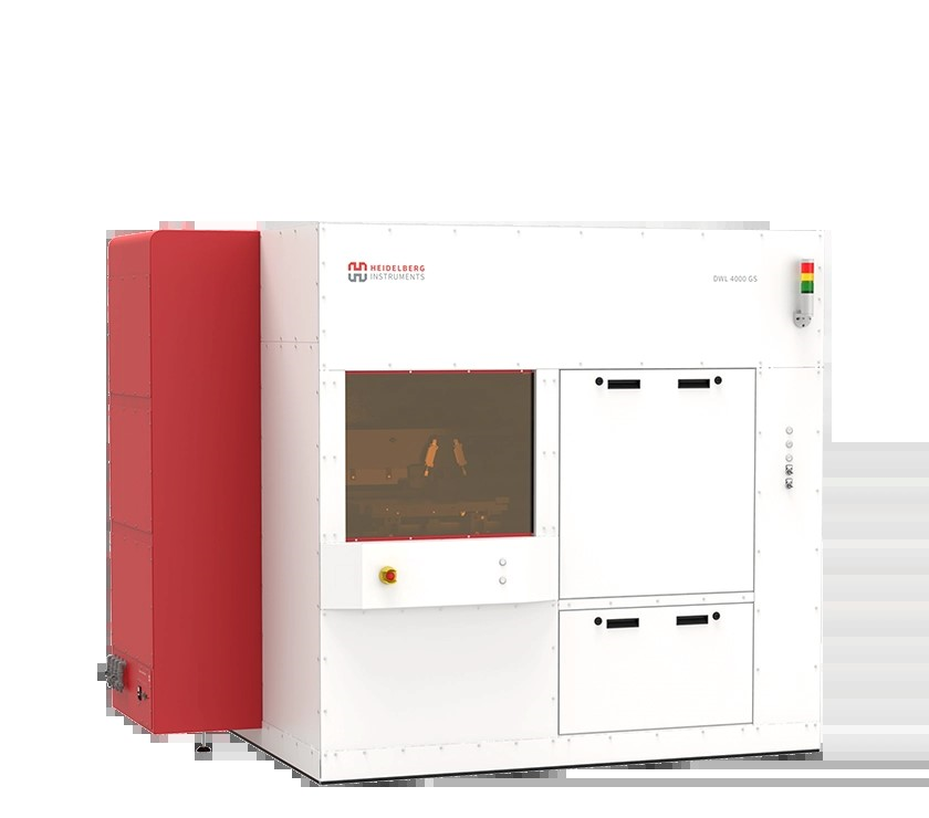
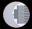
DWL 2000 GS / DWL 4000 GS
The most advanced industrial grayscale lithography tool on the market.
• Fast and flexible high-resolution pattern generators.
• Optimized for industrial-level Grayscale Lithography
• Designed for high-throughput patterning of masks and wafers
• For integrated circuits, MEMS, micro-optic and microfluidic devices, sensors, holograms, and security features on banknotes and ID cards.
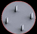
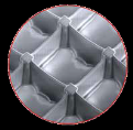
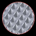
• Patterning of complex 2.5D structures in thick photoresist over large areas.
• Suitable for wafer-level micro-optics used for telecommunications, illumination, and industrial display manufacturing, as well as for device fabrication in life sciences.
For more information, please click here.
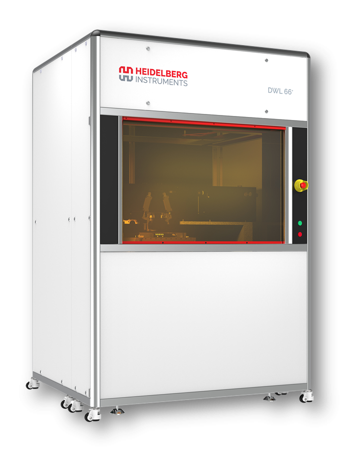
DWL 66⁺
Most versatile system for research and prototyping with variable resolution and wide selection of options.
• High-resolution direct-write pattern generator.
• Choice of 6 write modes with 2 laser wavelengths
• Ideal for research and development (R&D) in microelectronics, MEMS, microfluidics, sensors, non-standard substrates, advanced packaging — virtually any academic application that requires microstructure fabrication.
• Stands out with its Grayscale Exposure Mode which creates complex 2.5D microstructures such as micro-optics for mobile applications, diffractive optical elements (DOE), computer-generated holograms, and structured surfaces.
• It is a highly flexible and customizable system that precisely matches the requirements of your applications.
• Key features of the DWL 66⁺ are a high-resolution mode, front- and backside alignment, absolute position calibration and an automatic loading system.
For more information, please click here.
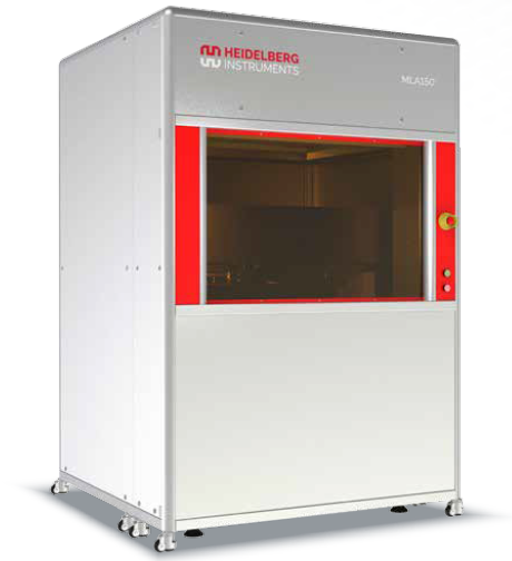
MLA 150
The fastest maskless aligner for R&D, rapid prototyping, and small production volumes.
• State-of-the-art Maskless Aligner Lithography tool.
• Fast automated front- and backside alignment procedures and outstanding speed.
• Areas of application include MEMS, micro-optics, diffractive optical elements, sensors, electronic components, and other devices for materials and life sciences.
For more information, please click here.
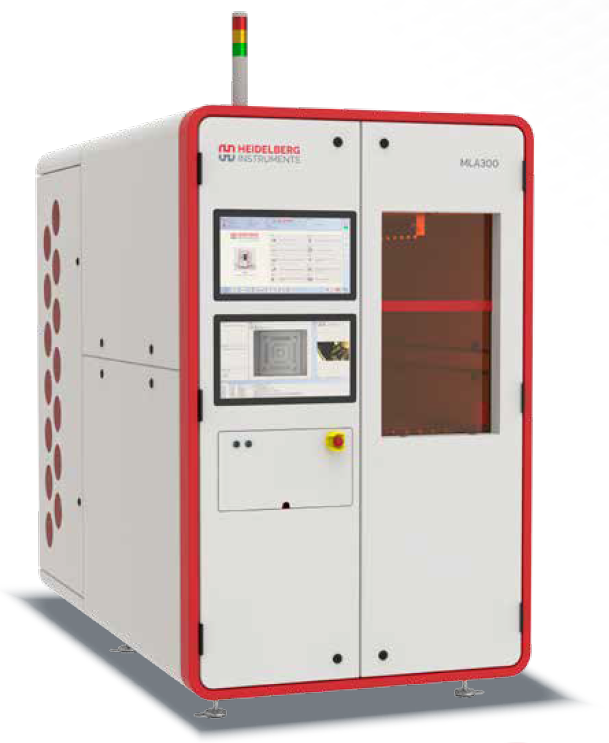
MLA 300
Optimized for flexible industrial production with highest precision and seamless integration into industrial production lines.
• High throughput, a simplified workflow, and integration with manufacturing execution systems (MES).
• Used for the production of sensors and sensor ICs, MEMS, and microfluidic devices.
• Full automation with customizable loading options, software designed for production environments, and patented substrate tracking technology.
• Modularity enables fast maintenance, replacement, or repair. Real-time autofocus compensates for substrate warp or corrugations, ensuring flawless patterning.
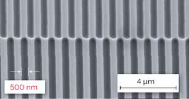
• High resolutions of 2 µm lines and spaces at the high throughput and high availability expected in production.
• Integration Customizable workflow “wizards” to start exposure jobs, and integration to a central MES via SECS/GEM or OPC-UA protocols.
For more information, please click here.
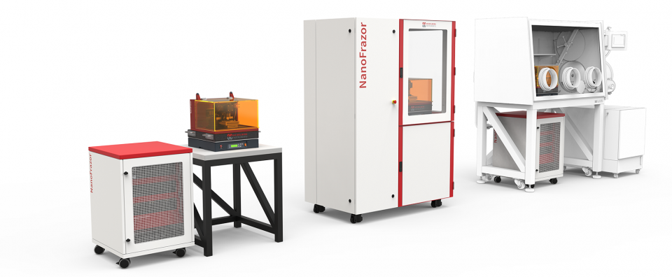
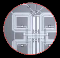
NanoFrazor
The versatile and modular nanolithography tool.
• Groundbreaking commercial system for Thermal Scanning Probe Lithography(t-SPL).
• Easy patterning of nanostructures even with complex geometries; minimum lateral features 15 nm, vertical resolution 2 nm.
• Markerless overlay and stitching accuracy 25 nm specified, sub-10 nm overlay shown.
• Areas of application include Quantum devices, 1D/2D materials, Photonics and Biotechnology.
For more information, please click here.
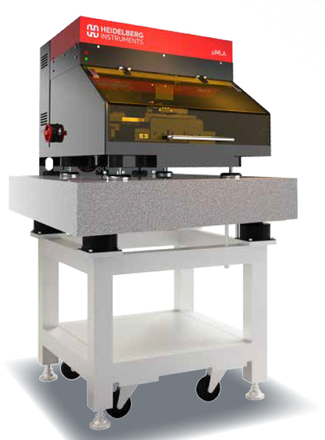

μMLA
Configurable and compact tabletop maskless aligner.
• State-of-the-art in maskless technology built on the renowned µPG platform.
• Entry-level research and development (R&D) tool for virtually any application requiring microstructures.
• Typical examples are Microfluidics, Micro Optics, Sensors, MEMS, and Material Science.
• Flexible and customizable tool.
For more information, please click here.
For more information, please visit www.heidelberg-instruments.com.