Semiconductor Equipment & Materials
Metrology & Inspection
AOI and Defect Inspection
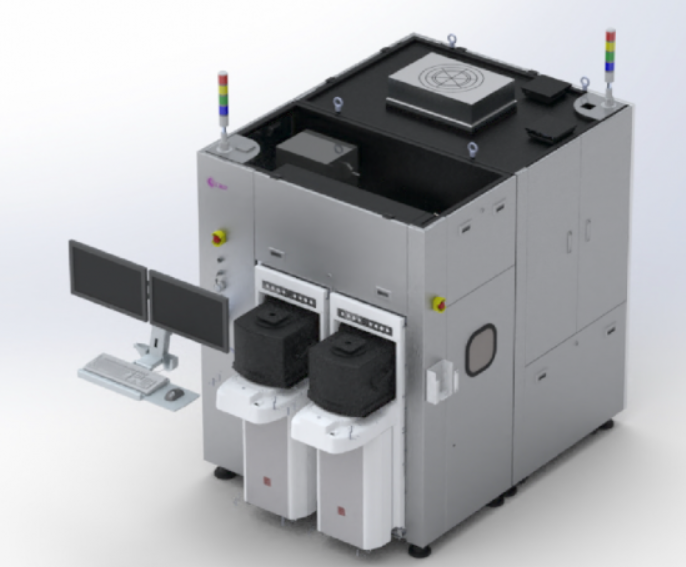
Buffalo S3002
Application
8, 12 inch wafer
Wafer incoming inspection (incoming material)
IQC, finished product outgoing inspection OQC
• 2.5D/3D IC
• Fan-out Wafer Level Packaging (FOWLP)
• Fan-out Panel Level Packaging (FOPLP)
Minimum detectable defect size: 1μm
Key flaws
• RDL Damage
• Pad Open
• Short
• Residue
• Particle
• Scratch
Key measurements
• RDL CD
• Pad Open CD
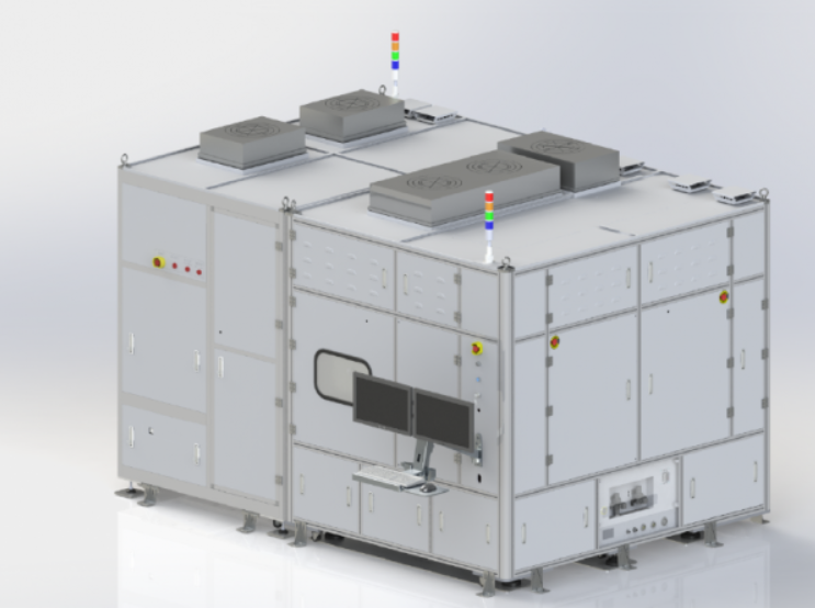
Buffalo 7002
Application
Panel 700*700mm
• FOPLP (Fan-out Panel Level Packaging)
Minimum detection size: 1μm
Key testing/measurement
• Open
• Short
• Nick
• Protrusion
• Cooper Void
• Pin Hole
• Cu Island
• Station on Die Surface
• Ti Remain
• Foreign Material
• Scratch on Copper Surface
• Dry Film Remain
• False Defect Rate