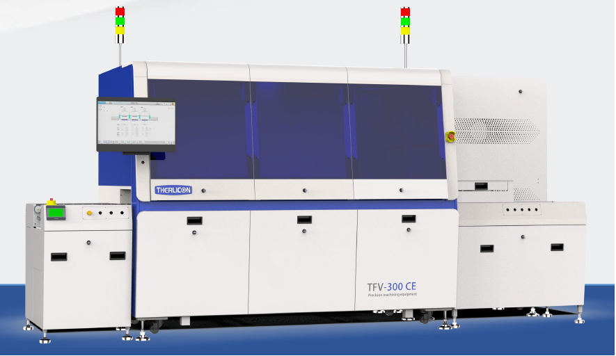
Semiconductor Equipment & Materials
Wafer Fabrication – Thin Film and Advanced Packaging Process
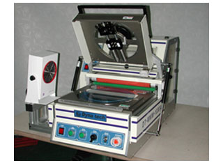
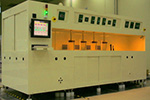
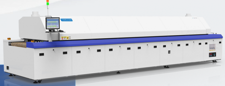
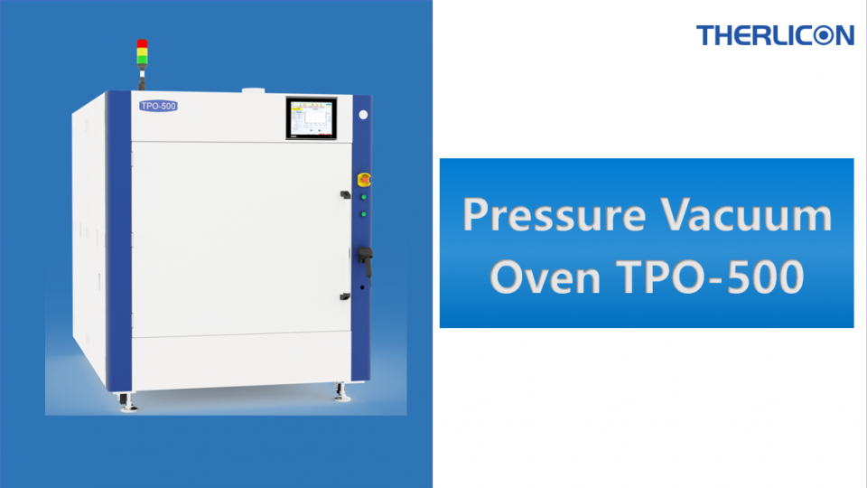
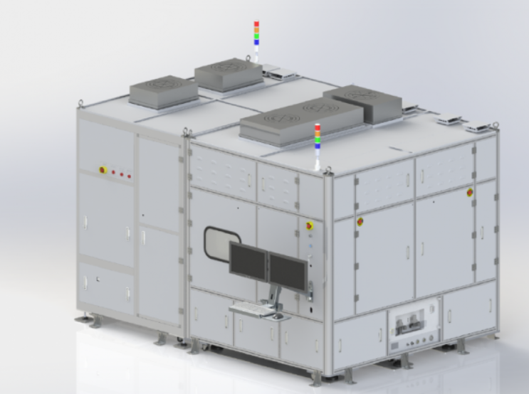
Wafer Processing Systems
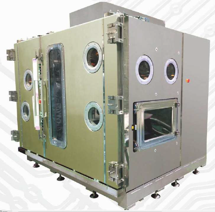
• Fully automatic wafer backgrind, mounting and de-tape system for 300mm ultra-thin wafer
• Stand alone Mounter, Detaper, Laminator of BSP/LC Tape, DAF Tape, BG & Dry Film
• UV irradiation, Manual Tape mount, De-tape, OCR Barcode print
• Wafer Transfer System, Debonder, Warpage Adjuster for eWLB process
For more information, please visit www.dynatech.co.kr.
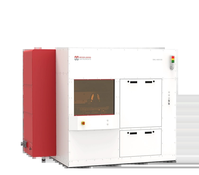
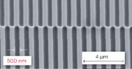
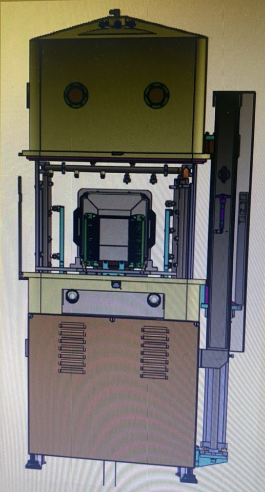
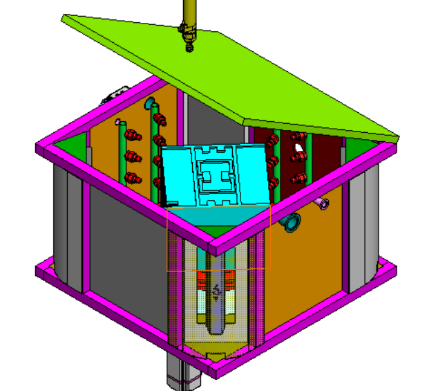
DWL 2000 GS / DWL 4000 GS
The most advanced industrial grayscale lithography tool on the market.
• Fast and flexible high-resolution pattern generators.
• Optimized for industrial-level Grayscale Lithography
• Designed for high-throughput patterning of masks and wafers
• For integrated circuits, MEMS, micro-optic and microfluidic devices, sensors, holograms, and security features on banknotes and ID cards.
• Patterning of complex 2.5D structures in thick photoresist over large areas.
• Suitable for wafer-level micro-optics used for telecommunications, illumination, and industrial display manufacturing, as well as for device fabrication in life sciences.
For more information, please click here.
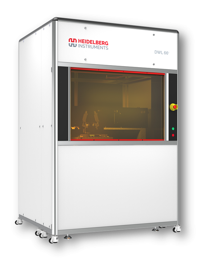
DWL 66⁺
Most versatile system for research and prototyping with variable resolution and wide selection of options.
• High-resolution direct-write pattern generator.
• Choice of 6 write modes with 2 laser wavelengths
• Ideal for research and development (R&D) in microelectronics, MEMS, microfluidics, sensors, non-standard substrates, advanced packaging — virtually any academic application that requires microstructure fabrication.
• Stands out with its Grayscale Exposure Mode which creates complex 2.5D microstructures such as micro-optics for mobile applications, diffractive optical elements (DOE), computer-generated holograms, and structured surfaces.
• It is a highly flexible and customizable system that precisely matches the requirements of your applications.
• Key features of the DWL 66⁺ are a high-resolution mode, front- and backside alignment, absolute position calibration and an automatic loading system.
For more information, please click here.
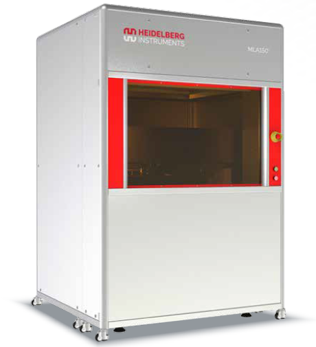
MLA 150
The fastest maskless aligner for R&D, rapid prototyping, and small production volumes.
• State-of-the-art Maskless Aligner Lithography tool.
• Fast automated front- and backside alignment procedures and outstanding speed.
• Areas of application include MEMS, micro-optics, diffractive optical elements, sensors, electronic components, and other devices for materials and life sciences.
For more information, please click here.
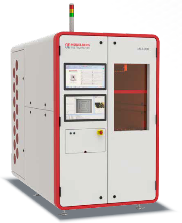
MLA 300
Optimized for flexible industrial production with highest precision and seamless integration into industrial production lines.
• High throughput, a simplified workflow, and integration with manufacturing execution systems (MES).
• Used for the production of sensors and sensor ICs, MEMS, and microfluidic devices.
• Full automation with customizable loading options, software designed for production environments, and patented substrate tracking technology.
• Modularity enables fast maintenance, replacement, or repair. Real-time autofocus compensates for substrate warp or corrugations, ensuring flawless patterning.
• High resolutions of 2 µm lines and spaces at the high throughput and high availability expected in production.
• Integration Customizable workflow “wizards” to start exposure jobs, and integration to a central MES via SECS/GEM or OPC-UA protocols.
For more information, please click here.
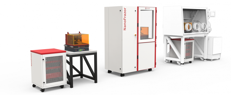
NanoFrazor
The versatile and modular nanolithography tool.
• Groundbreaking commercial system for Thermal Scanning Probe Lithography(t-SPL).
• Easy patterning of nanostructures even with complex geometries; minimum lateral features 15 nm, vertical resolution 2 nm.
• Markerless overlay and stitching accuracy 25 nm specified, sub-10 nm overlay shown.
• Areas of application include Quantum devices, 1D/2D materials, Photonics and Biotechnology.
For more information, please click here.
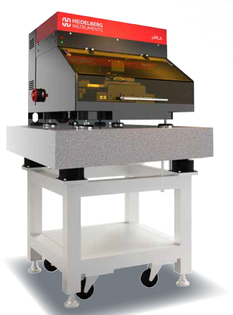

μMLA
Configurable and compact tabletop maskless aligner.
• State-of-the-art in maskless technology built on the renowned µPG platform.
• Entry-level research and development (R&D) tool for virtually any application requiring microstructures.
• Typical examples are Microfluidics, Micro Optics, Sensors, MEMS, and Material Science.
• Flexible and customizable tool.
For more information, please click here.
For more information, please visit www.heidelberg-instruments.com.
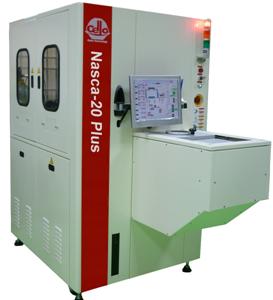
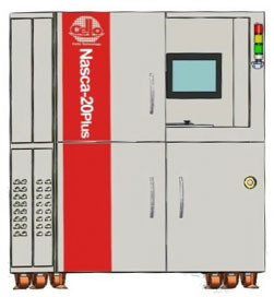
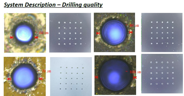
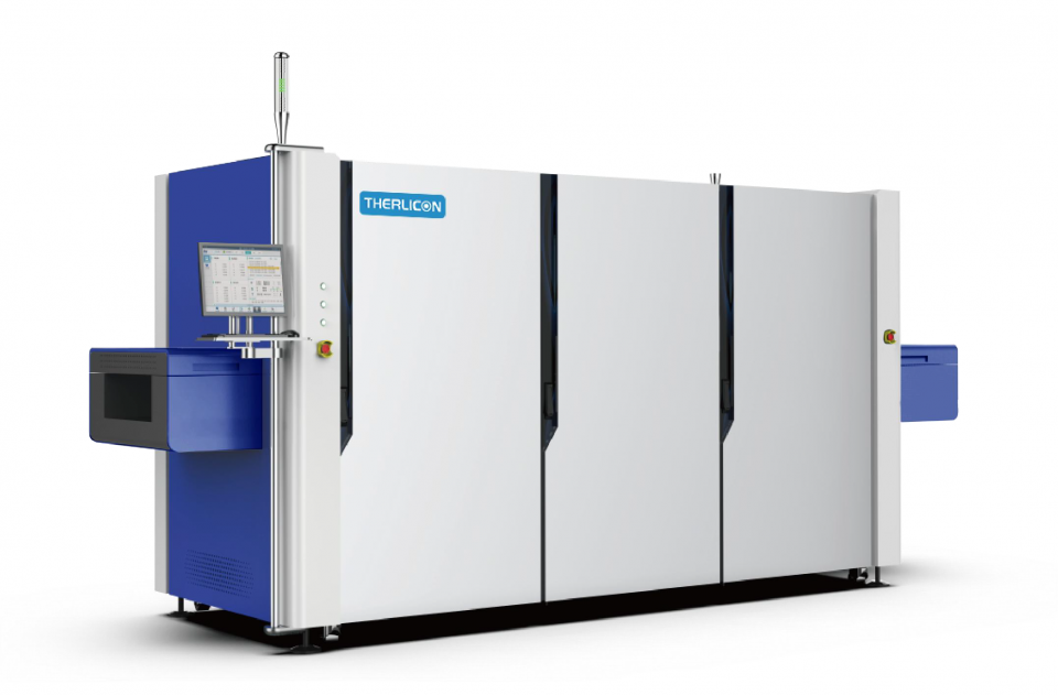
Nasca-20 Plus, ICP-RIE
APPLICATIONS
• Anisotropic etching of silicon films for ULSI devices.
• Etching of metal films.
• Etching of GaAs, GaN, InP and other Compound semiconductor films.
• Silicon Deep etching (MEMS).
• Production of waveguide devices.
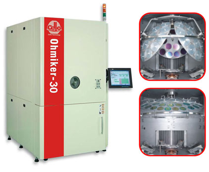

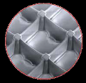
Ohmiker-30
Model Diamond Thermal and Electron Beam Evaporator, high-capacity manufacturing model
Fully automatic with manual override system for 2” to 12” wafer in a compact footprint. The Thermal & Electron Beam Evaporation System is designed for conformal and lift-off deposition process of thin film metal.
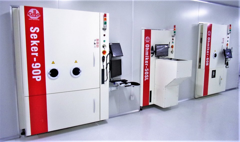
Sputter & ICP Equipment
Seker-90P: Optical Coater
Ohmiker-50SL: Sputter
Ohmiker-60B: Evaporator
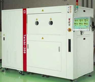
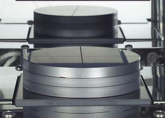
Tacichi-306
Wafer Bonder
Batch Type Process Equipment
Batch type process for Dry Film strip, Photoresist Strip, Glass Slim/Etch, Wafer Clean, Electroplating ECD.
Frontend Wafer Fabrication Process Equipment
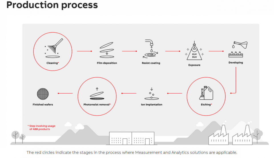
1. EUV Mask Clean
2. Prime Wafer Clean
3. Wafer Stress Release Etch
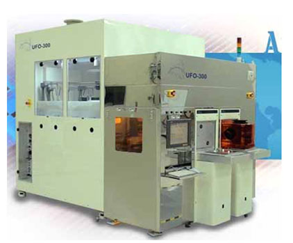
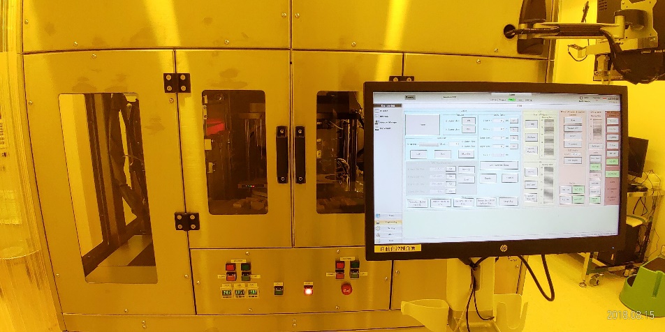
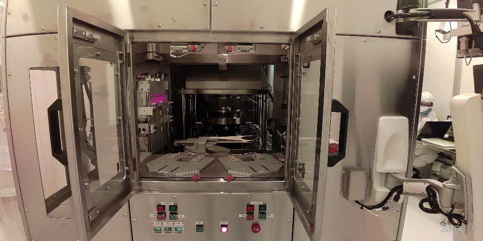
UFO-300
UFO-300 model is a Single Wafer Process system for 200 - 300mm wafers, and is capable of performing UBM Etch, Photoresist Strip, Wafer Clean/Scrub, Metal Lift-Off, PER Polymer Remover and Solder & Flux Clean.


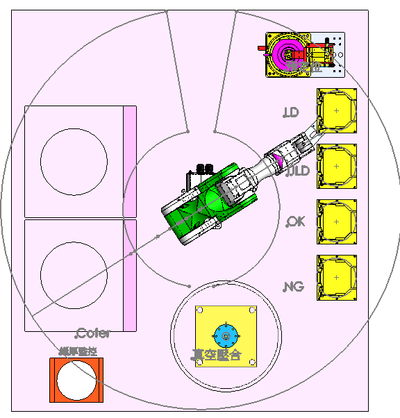

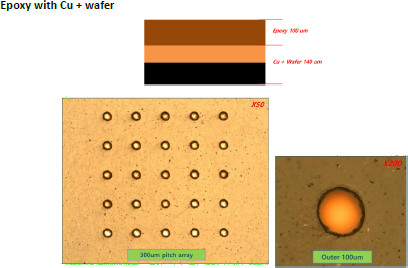

Vacuum Lamination Process
MCK's vacuum lamination technology can offer:
• Bubble-free film lamination
• Significant improvement in yield stability
• Proven track record in glass-based substrate processes


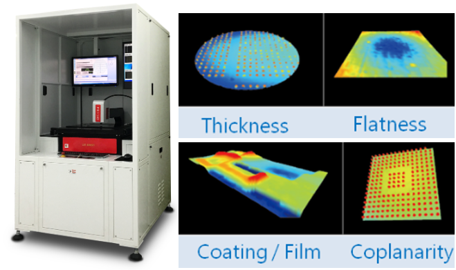
Metrology & Inspection
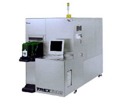
TREX 630
The TREX 630 series is for 200mm or 300mm wafers and may be configured for lab or in-line use. This system's high-uptime, low maintenance configuration have already been selected by a large majority of the 300mm fabs world wide. This series may be configured a number of ways, from a powerful single sealed tube system to a powerful quad-source sealed tube configuration.
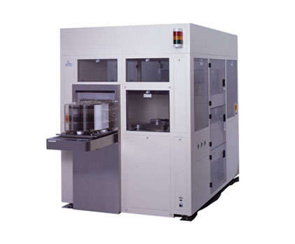
TVD-910
The Technos TVD-910 completely automates the vapor phase decomposition (VPD) prep for wafers. By dissolving the top oxide layer and concentrating the surface, it offers the ultimate in sensitivity for trace metal analysis. This versatile tool can prepare the droplet for analysis by placing it in a vial for inductively coupled mass spectrometry (ICP-MS) or drying the droplet on the surface of the wafer for total reflective X-ray fluorescence (TXRF).
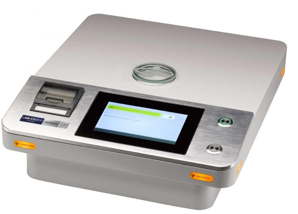
Bulk Analysis
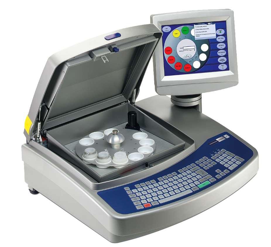
Lab-X5000 and X-Supreme8000 ED-XRF for petroleum, cement, and mining applications.
1. Lab-X5000
2. X-Supreme8000
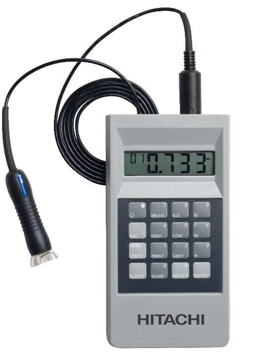
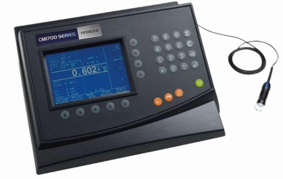
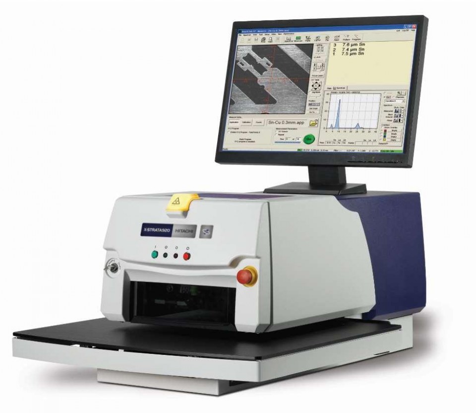
Coating Thickness Gauge
X-Strata920 SDD and CMI Series for Coating thickness, Micro-Spot Electronic Coating, Metal finishing, Precious metal applications.
1. CMI 200 Series
2. CMI 700 Series
3. X-Strata920 SDD
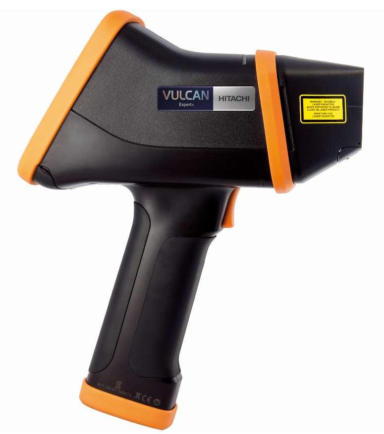
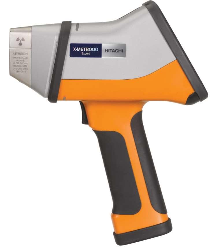
Industrial Analysis Products
Portable ED-XRF and LIBS for quick material analysis for RoHS, Recycling, PMI and Mining applications.
1. Vulcan Series
2. X-MET8000 Series
For more information, please visit hha.hitachi-hightech.com/en/.
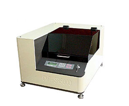

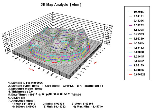
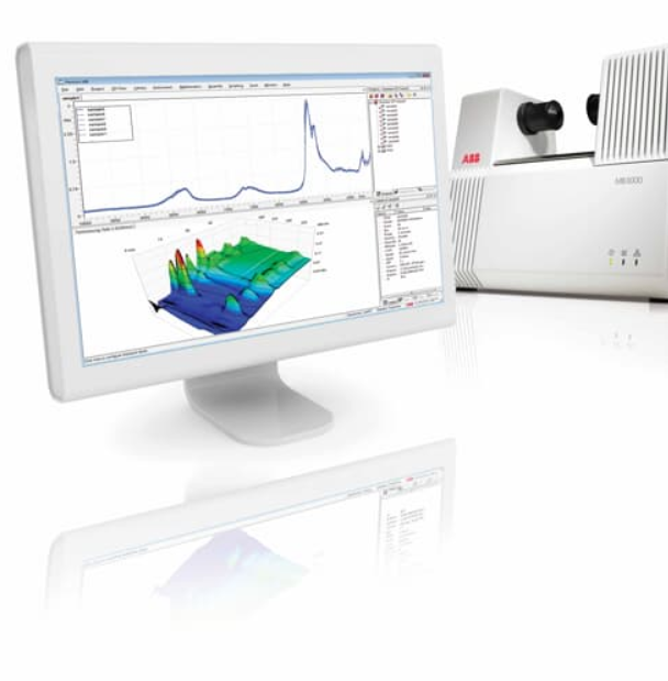
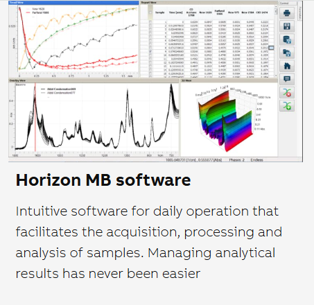
CMT-SR5000
The CMT-SR5000 is a high precision Four Point Prone system equipped to measure the Sheet Resistance and Resistivity of Silicon Wafer. This system is designed for easy operation by a personal computer with exclusive software, and this software has functions for various data analyses mapping and so on.
For more information, please visit www.fpp.co.kr.
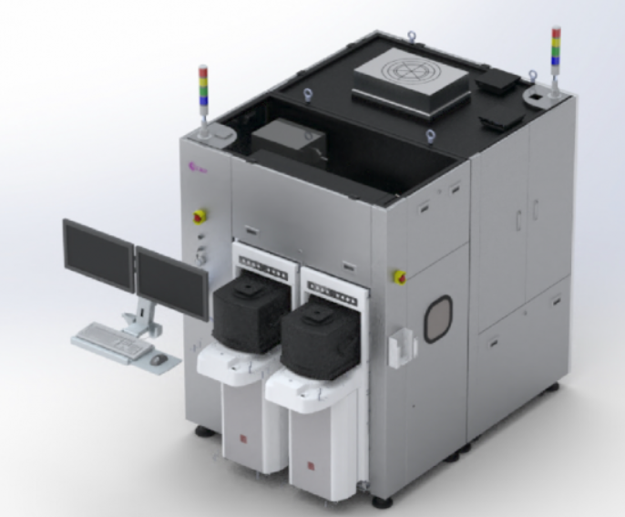
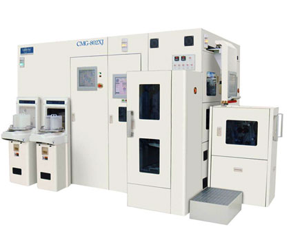
Buffalo S3002
Application
8, 12 inch wafer
Wafer incoming inspection (incoming material)
IQC, finished product outgoing inspection OQC
• 2.5D/3D IC
• Fan-out Wafer Level Packaging (FOWLP)
• Fan-out Panel Level Packaging (FOPLP)
Minimum detectable defect size: 1μm
Key flaws
• RDL Damage
• Pad Open
• Short
• Residue
• Particle
• Scratch
Key measurements
• RDL CD
• Pad Open CD
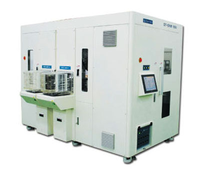
Buffalo 7002
Application
Panel 700*700mm
• FOPLP (Fan-out Panel Level Packaging)
Minimum detection size: 1μm
Key testing/measurement
• Open
• Short
• Nick
• Protrusion
• Cooper Void
• Pin Hole
• Cu Island
• Station on Die Surface
• Ti Remain
• Foreign Material
• Scratch on Copper Surface
• Dry Film Remain
• False Defect Rate
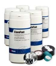
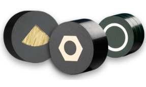
QRA & Materialographic Preparation
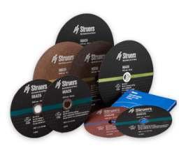
Consumables
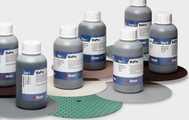
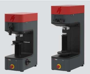
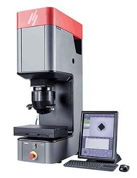
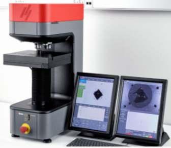
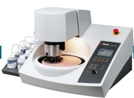
Hardness Testing

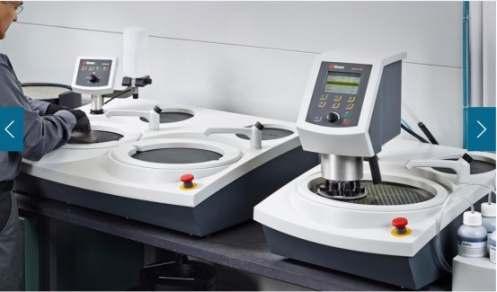
Materialographic Sample Preparation
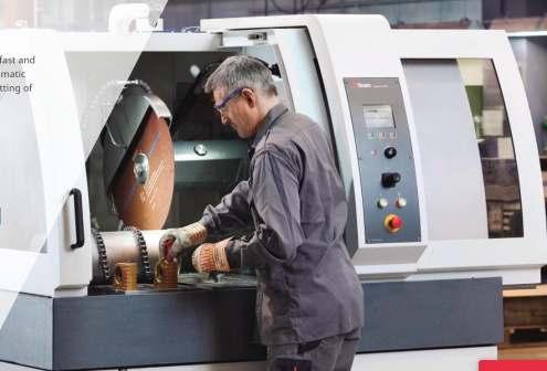
1. Cutting Machine
2. Precision cutting machine
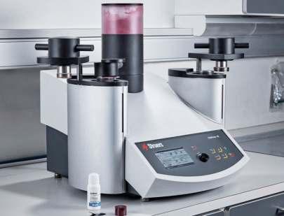
3. Hot Mounting
4. Vacuum Impregnation
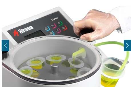
5-6. Grinding and Polishing
For more information please visit www.struers.com.
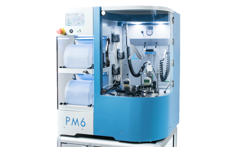
PM6
The PM6 machine is used extensively in the preparation of:
• Geological Thin Sections: i.e. Rock lapping system
• Semiconductor Materials i.e. Polishing silicon wafers
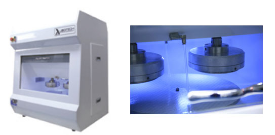
Tribo CMP System
Logitech’s CMP system offers nanometer level material removal capabilities on either individual die or wafers up to 200mm diameter.
This system is particularly suitable for the following specific applications:
• Silicon wafer CMP to <1nm Ra
• Global CMP of III-V Compound Semiconductor
• Global CMP of brittle, friable IR material substrates
• Global CMP of Sapphire, Gallium Nitride & Silicon Carbide substrates
• Reclamation of EPI ready substrates
• Final Stage thinning of SOS & SOI wafers to below 20 microns
• Device delayering for reverse engineering of FA applications
For more information, please visit www.logitech.uk.com.
Specialty Chemicals & Consumables
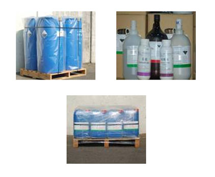
Specialty Materials
• RDL, Wafer Bump Process Specialty Etchants
Ti, TiW, Cu, Au, NiV, Si, Al, Ni, Cr, SiO2, Si3N4, Rework solutions
• Photoresist Strip or Polymer Removal Material
Positive & Negative Photoresist stripper, Thick Liquid and Dry Films stripper
• Gold Plating Solution
Non-cyanide gold solution, Reclaim service
• Photoresist Material
Positive and Negative. Application for FPD, LED and IC Fabrication.

Tape Material for Packaging Process
Polyimide tape, UV dicing tape, double sided tape
Customization service for high volume consumption
1. Backgrind tape
2. UV tape
3. Double Sided tape
4. High Temperature tape
5. Tape to tape transfer/ Re-taping process tape
6. Pre-cut tape
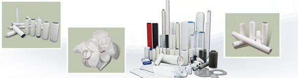
Semiconductor Grade Filtration Solutions
1. Semiconductor grade filtration solution
2. Electronics manufacturing grade filtration solution
3. Medical/pharmaceutical grade filtration solution
4. Food and beverage grade filtration solution
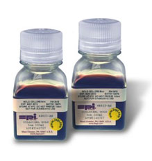
Colloidal Gold
SPI-Mark unconjugated gold colloidal suspensions are of outstanding EM quality.
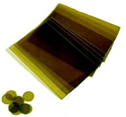
MICA Sheet
The highest quality for thin film deposition, replication and AFM studies.
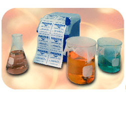
Parafilm(R) M
A unique self-sealing, moldable and flexible film for numerous uses in the typical laboratory, including the electron microscope laboratory.
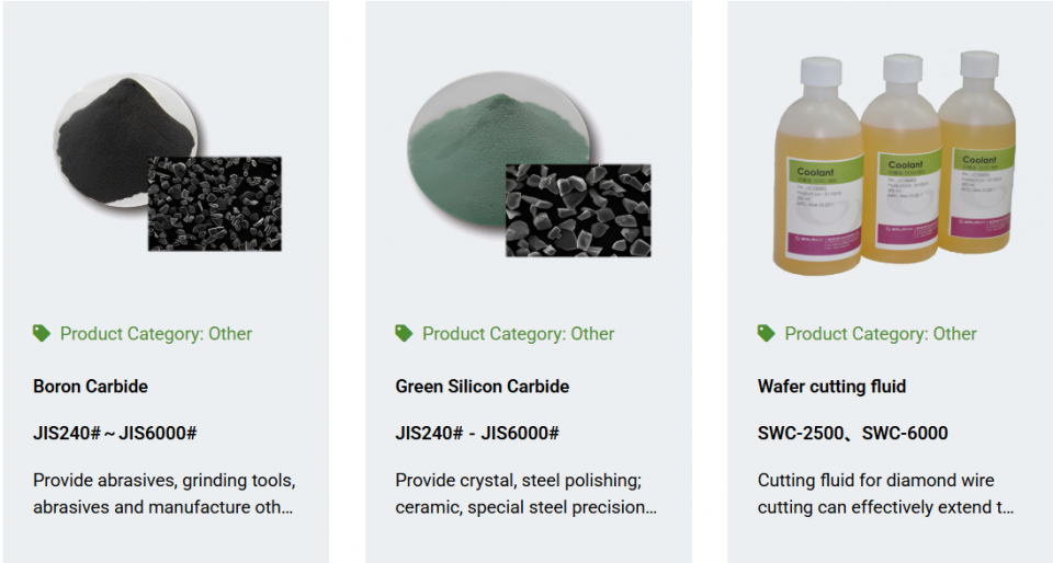
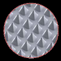
CMP and Slurry Materials
Boron Carbide
Green Silicon Carbide
• JIS240# - JIS6000#
• Provide abrasives, grinding tools, abrasives and manufacture other...
Wafer Cutting Fluid
• SWC-2500, SWC-6000
• Cutting fluid for diamond wire cutting can effectively extend the...
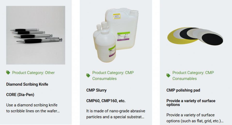
Diamond Scribing Knife
• CORE (Dia-Pen)
• Use a diamond scribing knife to scribble lines on the wafer...
CMP Slurry
• CMP60, CMP160, etc.
• It is made of nano-grade abrasive particles and a special substrate...
CMP Polishing Pad
• Provide a variety of surface options (such as flat, grid, etc.)
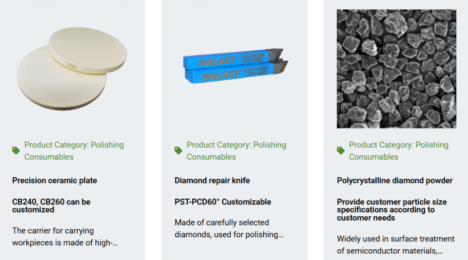
Precision Ceramic Plate
• CB240, CB260 (Customisable)
• The carrier for carrying workpieces is made of high-...
Diamond Repair Knife
• PST-PCD60° (Customisable)
• Made of carefully selected diamonds, used for polishing...
Polycrystalline Diamond Powder
• Provide customer particle size specifications according to customer needs
• Widely used in surface treatment of semiconductor materials...
Software
2. MES Host

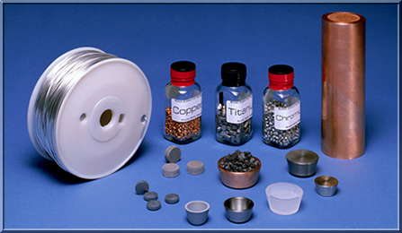
Specialty Materials
Sputter Targets, E-Beam Materials

UTI Stepper Parts & Equipment Repair and Exchange
Supports customer in refurbished UT stepper equipment, parts and contract service. Offers a range of specialty materials like Silicon Wafers, Targets/Crucibles and Integrate Small Systems for the semiconductor market.
• For model 990, 1000, 1100, 1500, 1700, 1900 Ultratech steppers
• Available sizes: 3", 4", 5", 6" for round substrates
• Fully refurbished and operational
• Demonstration can be conducted in our facility in Rocklin, Ca.
Wafers & Plates
Silicon Wafer, Glass Wafer, Quartz Carrier, Sapphire Plate